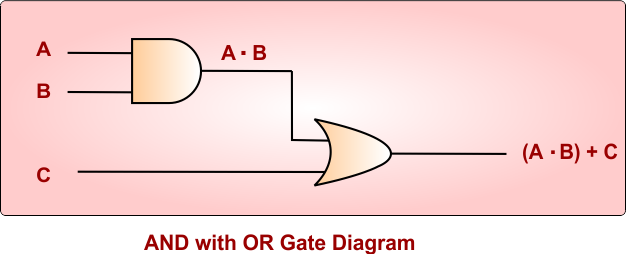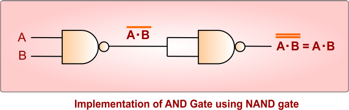












AND Logic Gate
The AND logic gate is a basic logic gate that gives an output of 1 (High) when at all inputs are “1”. It gives the output 0 (Low) when at least one input is “0”
AND Gate Boolean Expression
The Boolean expression of AND logic Gate is given below
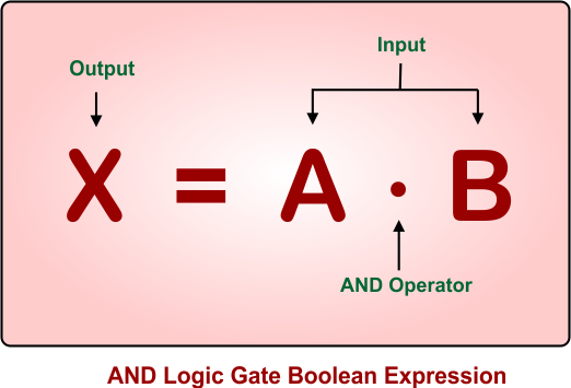
where
A, B are the inputs, A.B is the output, and “.” is the operator for AND Gate
AND Logic Gate Symbols
Here are standard diagrams that show the symbol of AND logic gate. The number of inputs to a AND logic gate can be different according to the requirement
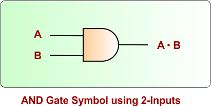
AND Gate Symbol for 2 Inputs
In the following AND gate diagram, A and B are the inputs, and A.B is the output
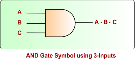
AND Gate Symbol for 3 Inputs
In the following AND gate diagram, A, B, and C are the inputs, and A.B.C is the output
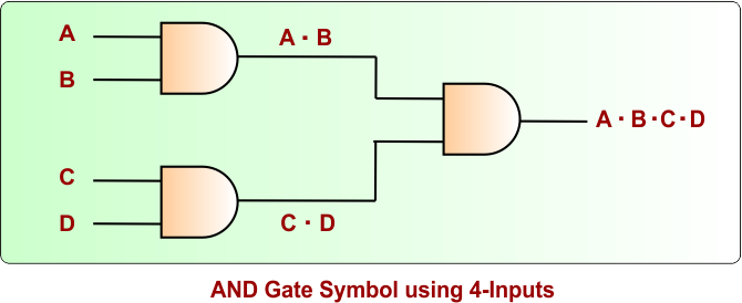
AND Gate Symbol for 4 Inputs
In the following AND gate diagram, A, B, C, and D are the inputs, and A.B.C.D is the output
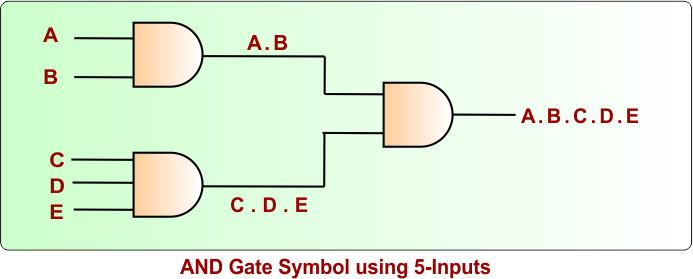
AND Gate Symbol for 5 Inputs
In the following AND gate diagram, A, B, C, D, and E are the inputs, and A.B.C.D.E is the output
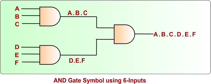
AND Gate Symbol for 6 Inputs
In the following AND gate diagram, A, B, C, D, E, and F are the inputs, and A.B.C.D.E.F is the output
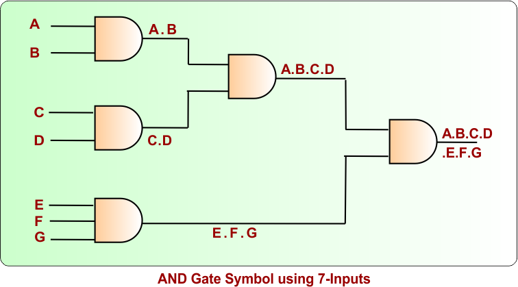
AND Gate Symbol for 7 Inputs
In the following AND gate diagram, A, B, C, D, E, F, and G are the inputs, and A.B.C.D.E.F.G is the output
AND Gate Equivalent Circuit
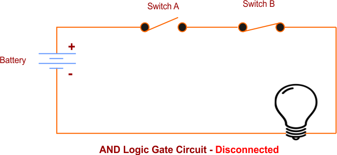
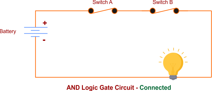
AND Logic Gate can also be represented using an electrical circuit. In this circuit, two switches are connected in Series.
Case 01: If either one or both switches are OFF (disconnected), the lamp will not light up as shown in the following AND Logic gate diagram
Case 02: The lamp remains ON only when both switches are ON (connected), as shown in the following AND Logic gate diagram
AND Logic Gate Truth Table
Truth table shows all possible input combinations and their corresponding outputs for a logic gate. AND Logic Gate truth tables for different numbers of inputs are given below
|
The number of possible input combinations in a truth table is calculated using 2ⁿ, where n represents the number of inputs. For example:
|
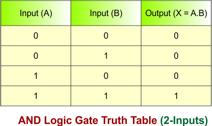
AND Logic Gate Truth Table for 2 inputs
AND Logic Gate Truth Table for two inputs (A, B) is given below
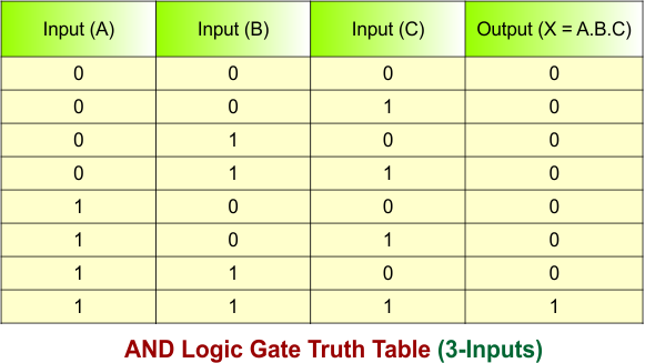
AND Logic Gate Truth Table for 3 inputs
AND Logic Gate Truth Table for three inputs (A, B, C) is given below
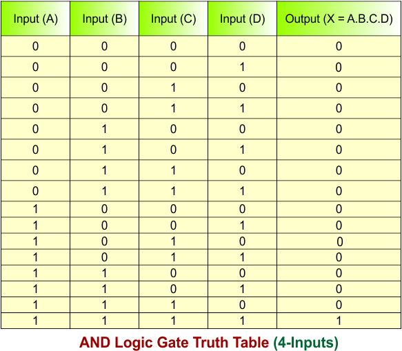
AND Logic Gate Truth Table for 4 inputs
AND Logic Gate Truth Table for four inputs (A, B, C, D) is given below
AND Gate Circuit Diagram Using Transistors
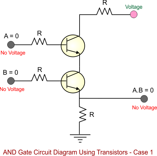
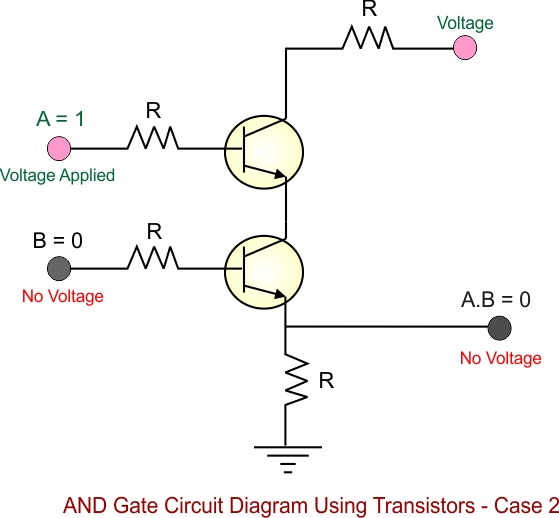
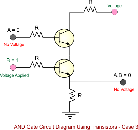
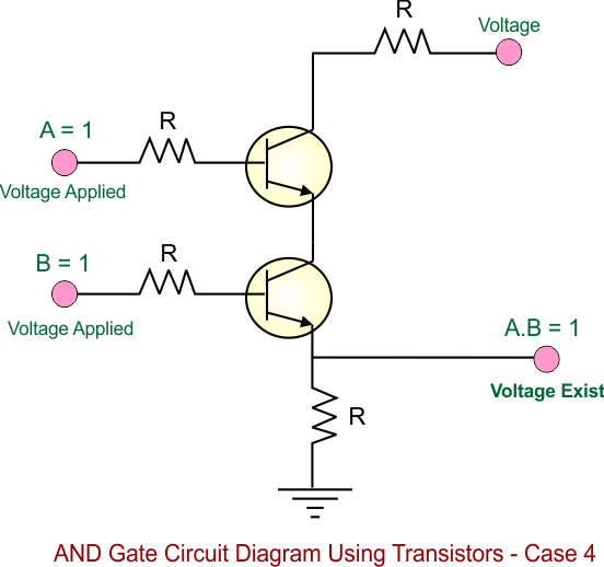
An AND Logic Gate can be constructed using transistors; an NPN transistor is mainly used in simple circuit construction. This NPN circuit uses two inputs; if either input is Low (0), it produces an output (0), which is the basic principle of an AND logic gate.
|
Very Important: In an NPN transistor, applying voltage to the collector alone does not turn the transistor ON. The transistor requires a base current to allow current to flow from the collector to the emitter. |
Let’s discuss AND Logic Gate circuit using NPN transistors, where two inputs (A, B)
Case 01: When A = 0, B = 0, then no current is applied to either transistor’s base, so both transistors remain OFF, and the output is 0.
Case 02: When A = 1, B = 0, then no current is applied to the base of transistor B, so transistor B remains OFF, and the output is 0.
Case 03: When A = 0, B = 1, then no current is applied to the base of transistor B, so transistor A remains OFF, and the output is 0.
Case 04: When A = 1, B = 1, then current is applied to the bases of both transistors, turning both ON, and the output remains 1.
AND Logic Gate with NOT Gate
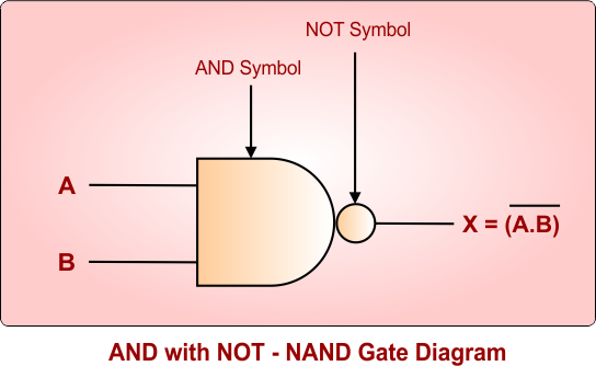
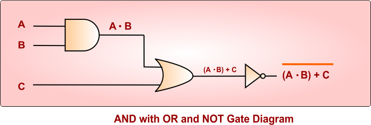
When we use NOT gate with AND Gate, it revert the output of AND Gate. This Combination is known as NAND Gate. First AND operation is performed and then NOT gate reverse the output of AND Gate.
The following diagram shows the very basic AND with Not logic circuit