












4 Input NAND Gate
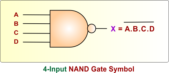
A 4-input NAND gate is a digital logic gate with 4 inputs and 1 output.
- The output is LOW (0) when all four inputs are HIGH (1).
- The output is HIGH (1) when at least one input is LOW (0).
Example: For four inputs, there will be 4 variables (i.e., A, B, C, and D) and the output is represented by the variable X. The Boolean expression for a 4-input NAND logic gate is X = (A · B · C · D)’.
Let’s explain the 4-input NAND logic gate symbol, Boolean expression, and Truth Table.
4-Input NAND Gate Symbol
The 4-input NAND logic gate symbol has four input terminals, represented by A, B, C, and D. The output is represented by X.
4-Input NAND Gate Boolean Expression
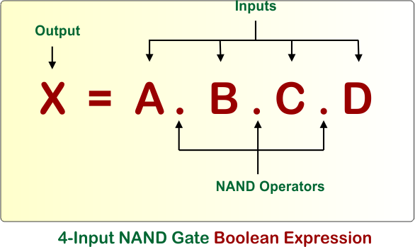
The Boolean expression of a 4-input NAND gate with inputs A, B, C, and D and output X is:
- X = (A · B · C · D)’
Here, the “·” symbol represents the AND operation, while the bar (‘) symbol represents the NOT operation. Therefore, a NAND gate performs the AND operation followed by NOT. The following diagram shows the Boolean expression of a 4-input NAND gate.
4-Input NAND Gate Truth Table
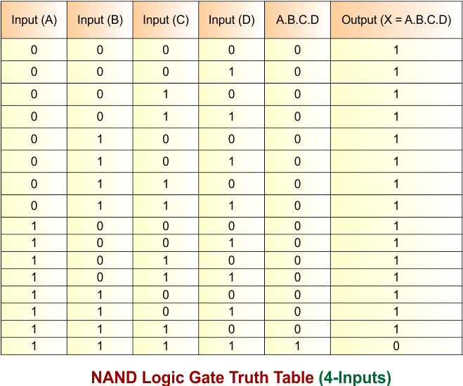
The 4-input NAND logic gate truth table shows the output for all possible combinations of the inputs A, B, C, and D. The output X becomes LOW (0) only when all four inputs are HIGH (1). If any input is LOW (0), the output becomes HIGH (1). The 4-input NAND gate has 2⁴ = 16 possible input combinations.
Let’s explain the truth table of a 4-input NAND logic gate.
- A = 0, B = 0, C = 0, D = 0: All inputs are LOW, so the output is 1 (HIGH).
- A = 0, B = 0, C = 0, D = 1: Inputs A, B, and C are LOW, so the output is 1 (HIGH).
- A = 0, B = 0, C = 1, D = 0: Inputs A, B, and D are LOW, so the output is 1 (HIGH).
- A = 0, B = 0, C = 1, D = 1: Inputs A and B are LOW, so the output is 1 (HIGH).
- A = 0, B = 1, C = 0, D = 0: Inputs A, C, and D are LOW, so the output is 1 (HIGH).
- A = 0, B = 1, C = 0, D = 1: Inputs A and C are LOW, so the output is 1 (HIGH).
- A = 0, B = 1, C = 1, D = 0: Inputs A and D are LOW, so the output is 1 (HIGH).
- A = 0, B = 1, C = 1, D = 1: Input A is LOW, so the output is 1 (HIGH).
- A = 1, B = 0, C = 0, D = 0: Inputs B, C, and D are LOW, so the output is 1 (HIGH).
- A = 1, B = 0, C = 0, D = 1: Inputs B and C are LOW, so the output is 1 (HIGH).
- A = 1, B = 0, C = 1, D = 0: Inputs B and D are LOW, so the output is 1 (HIGH).
- A = 1, B = 0, C = 1, D = 1: Input B is LOW, so the output is 1 (HIGH).
- A = 1, B = 1, C = 0, D = 0: Inputs C and D are LOW, so the output is 1 (HIGH).
- A = 1, B = 1, C = 0, D = 1: Input C is LOW, so the output is 1 (HIGH).
- A = 1, B = 1, C = 1, D = 0: Input D is LOW, so the output is 1 (HIGH).
- A = 1, B = 1, C = 1, D = 1: All inputs are HIGH, so the output is 0 (LOW).
4-Input NAND Gate – Timing Diagram
4-input NAND gate timing diagram showing the relationship between inputs A, B, C, D, and output X in a digital logic circuit. The diagram illustrates the logic-level transitions of four inputs (A, B, C, and D) and one output (X) over time.
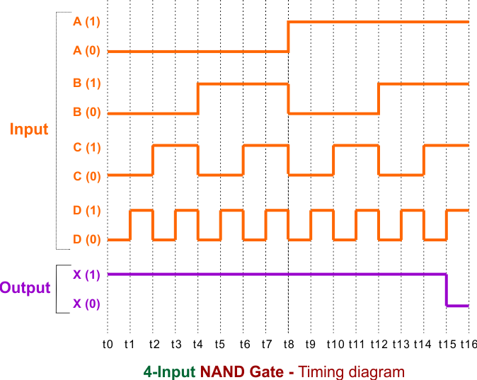
- Input A: Initially remains at logic 0, then changes to 1 midway through the timing interval and stays high.
- Input B: Alternates between logic 0 and 1 at longer time intervals.
- Input C: Toggles between 0 and 1 more frequently than A and B.
- Input D: Alternates between logic 0 and 1 at a different timing pattern.
- Output X: Remains at logic 1 whenever at least one input is 0. It changes to logic 0 only when A = 1, B = 1, C = 1, and D = 1.
The vertical dotted lines divide the diagram into equal time intervals, making it possible to compare the input transitions with the corresponding output behavior.