












NOT Logic Gate
A NOT logic gate takes only a single binary input and produces the output. It inverts or reverses the input that’s why it is also called an inverter.
- If the input is 1(HIGH), then the output will be 0 (LOW)
- If the input is 0(LOW), then the output will be 1 (HIGH)
It is different from OR and AND gates, because they take two binary inputs.
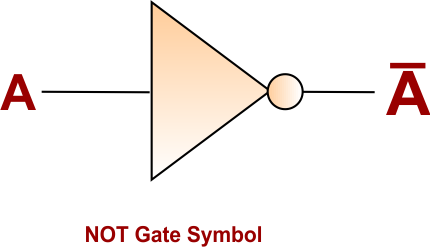
NOT Gate Symbol
NOT logic gate symbol looks like a triangle with a small circle, called a bubble, at the output. The following diagram shows the NOT gate symbol
Truth Table of NOT Gate
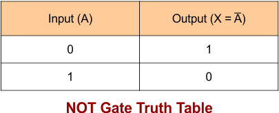
The input for the NOT gate is only one, so the NOT gate contains 21 = 2 possible input combinations. Where the input can either be 0 or 1. The following is the Truth Table for NOT gate, which shows the output, which is the reverse of its input.
Boolean Expression of NOT Gate
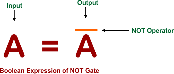
The following diagram shows the Boolean expression for the NOT gate, where the bar represents the NOT operation. Some other notations can also be used instead of the bar for the NOT gate.
NOT Gate Combined with Other Logic Gates
NOT gate reverses the output of another logic gate. When NOT logic gate is connected with the output of another logic gate, it produces the reverse of that gate’s output. The following Table expleain it
| Combination | Resulting Gate | Basic Definition |
|---|---|---|
| OR + NOT | NOR | Output of OR gate is reversed |
| AND + NOT | NAND | Output of AND gate is reversed |
| XOR + NOT | XNOR | Output of XOR gate is reversed |
| XNOR + NOT | XOR | Output of OR gate is reversed |
| NAND + NOT | AND | NOT reverses the NAND output and produces AND. |
| NOR + NOT | OR | NOT reverses the NOR output and produces OR. |
Let Explain each NOT Gate combination with Other Logic Gates
1. OR Gate Combined with NOT Gate
The OR gate first produces its output, and the NOT gate reverses it. This combination is called NOR Gate. The following diagram shows the regular expression, and it’s diagram when OR gate combined with NOT Gate.
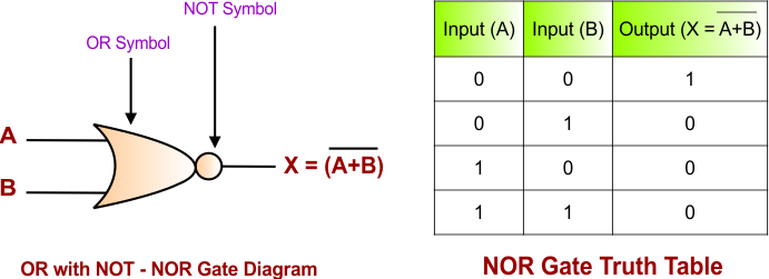
Hence, the output of NOR is the opposite of the OR gate.
2. AND Gate Combined with NOT Gate
The AND gate first produces its output, and the NOT gate reverses it. This combination is called NAND Gate. The following diagram shows the regular expression, and it’s diagram when NAND gate combined with NOT Gate.
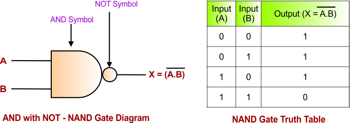
Hence, the output of NAND is the opposite of the AND gate.
3. XOR Gate Combined with NOT Gate
The XOR gate first produces its output, and the NOT gate reverses it. This combination is called XNOR Gate. The following diagram shows the regular expression, and it’s diagram when XOR gate combined with NOT Gate.
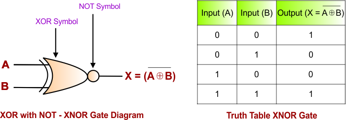
Hence, the output of XNOR is the opposite of the XOR gate.
4. XNOR Gate Combined with NOT Gate
The XNOR gate first produces its output, and the NOT gate reverses it. This combination is called XOR Gate. The following diagram shows the regular expression, and it’s diagram when XNOR gate combined with NOT Gate. Hence, the output of XOR is the opposite of the XNOR gate.
5. NAND Gate Combined with NOT Gate
The NAND gate first produces its output, and the NOT gate reverses it. This combination is called AND Gate. The following diagram shows the regular expression, and it’s diagram when NAND gate combined with NOT Gate. Hence, the output of AND is the opposite of the NAND gate.
6. NOR Gate + NOT Gate = OR Gate
The NOR gate first produces its output, and the NOT gate reverses it. This combination is called OR Gate. The following diagram shows the regular expression, and it’s diagram when NOR gate combined with NOT Gate. Hence, NOR + NOT = OR.
Implementation of NOT Gate Using Other Logic Gates
The case when we want to implement the NOT gate, but NOT gate is not available for the circuit becuase of any reason, then availabilty of any of the following gate is sufficient to implement NOT Gate
- NAND Logic Gate
- NOR Logic Gate
- XOR Logic Gate
- XNOR Logic Gate
| Important:
Only AND or OR gates are not sufficient to implement the NOT gate. But only NAND, NOR, XOR, or XNOR are sufficient to implement the NOT gate. |
Let’s discuss all cases of NOT gate implementations when NOT gate itself is not available
1. NOT Gate Using NAND Gate
NAND gate can be easily implemented as a NOT gate by connecting both inputs together.
Y = (A · A)̅
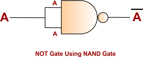
Since A · A = A, therefore X = A̅ is the output. This is the similar output which NOT gate generates. So single NAND gate is sufficient to implement a NOT gate.
2. NOT Gate Using NOR Gate
NOR gate can be easily implemented as a NOT gate by connecting both inputs together.
Y = (A+A)̅
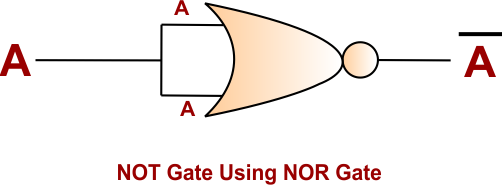
Since A + A = A, therefore X = A̅ is the output. This is the similar output which NOT gate generates. So single OR gate is sufficient to implement a NOT gate.
3. NOT Gate Using XOR Gate
An XOR gate can be used to implement a NOT gate by connecting one input to 1.
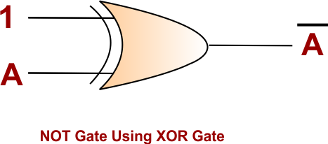
An XOR gate produces 1 when its inputs are different. Therefore, fix input A = 1, and B can alternate (0 or 1)
- If Input B = 0, then Output X = 1
- If Input B = 1, then Output X = 0
4. NOT Gate Using XNOR Gate
An XNOR gate can be used to implement a NOT gate by connecting one input to 0.
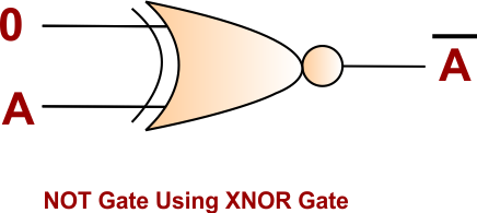
An XNOR gate produces 1 when its inputs are the same.
Therefore: Fix input A = 0, and B can alternate (either 0 or 1)
- If Input B = 0, then Output X = 0
- If Input B = 1, then Output X = 1
NOT Gate Using Transistor
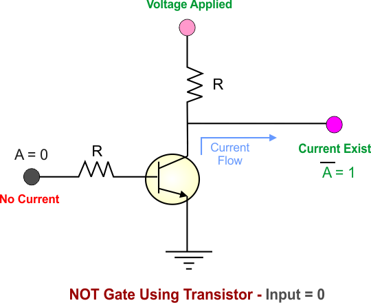
A NOT gate can also be built using a transistor-based circuit. In a simple transistor inverter, the transistor changes its output state according to the input signal.
NOT gate can also be implemented using a transistor-based circuit. A simple transistor inverter changes the binary input from 0 to 1 and 1 to 0.
In the case of a transistor inverter,
Case 01: When the input is 0, the transistor remains 0, and the output is 1.
Case 02: When the input is 1, the transistor turns 1 and the output becomes 0.
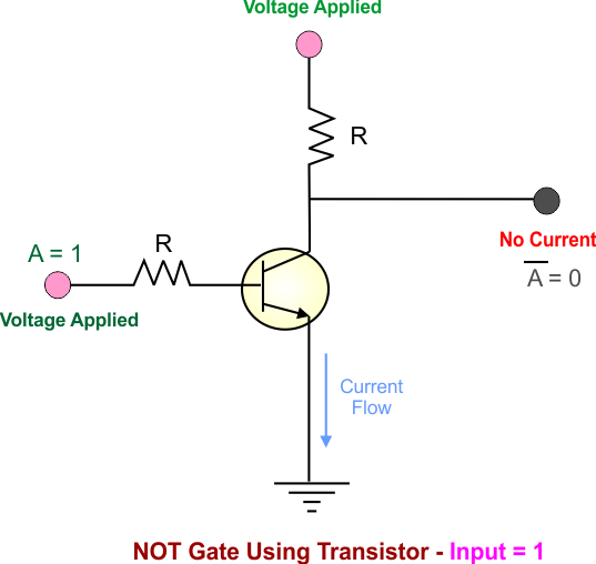
Thus, the transistor-based circuit generates the reverse of the input, which is the basic operation of a NOT gate.
NOT Gate Using Circuit Switch
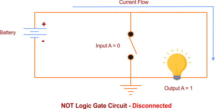
NOT logic gate can be understood by using a simple switch circuit. NOT gate gives an output that is the reverse of the input. The following diagram shows the bulb example
Case 01: Switch Open (Input = 0): The output lamp is ON (Output = 1).
Case 02: Switch Closed (Input = 1): The circuit redirects or bypasses the current, so the output lamp becomes OFF (Output = 0).
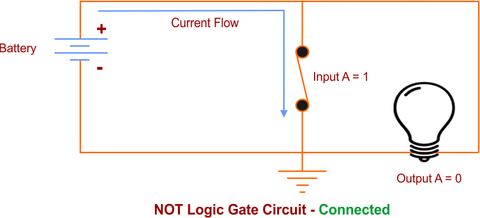
Therefore, the switch circuit works like a NOT gate because it inverts the input signal
Applications of NOT Gate
NOT logic gate is mainly used in digital electronic circuit, here are some common applications
- Signal inversion: Converts a HIGH signal into LOW and vice versa.
- Control circuits: Produces an opposite control signal when required.
- Digital systems: Used to create more complex logic functions.
- Memory circuits: Used as part of different digital storage circuits.
- Computing circuits: Helps implement logical and arithmetic operations.
- Logic gate implementation: Used when an inverted signal is required.
NOT Gate vs Other Logic Gates
Here is a very basic table of all logic gates along with NOT logic gate
| Logic Gate | Number of Inputs | Basic Operation |
|---|---|---|
| NOT | 1 | Inverts the input |
| AND | 2 or more | Output is 1 when all inputs are 1 |
| OR | 2 or more | Output is 1 when at least one input is 1 |
| NAND | 2 or more | Inverted AND operation |
| NOR | 2 or more | Inverted OR operation |
| XOR | 2 or more | Output is 1 when inputs are different |
| XNOR | 2 or more | Output is 1 when inputs are the same |