


Common Bus System
This lecture will explain the common bus system with single-address instructions because the mechanism of a common bus system is best for single-address instructions rather than two or three-address instructions.
Purpose Of Common Bus System
A Common Bus system provides a path for transferring data between registers and memory or between registers.
Common Bus System Diagram
A common bus system connects seven components (six registers and one memory) to a common bus. So, to represent these seven components of the common bus system in binary, we require three select lines: S0, S1, and S2.
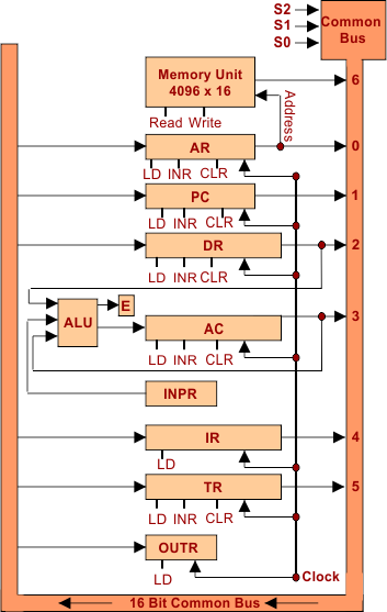
Essential Components of Common Bus SystemThe input register (INPR) and the output register (OUTR) send and receive data character by character. Eight bits are required to represent a character. So, INPR and OUTR registers needed 8 bits. These registers communicate with the 8-least significant bits on the common bus
How Common Bus System Works?
Step I: Any register can send data to a common bus by activating its selected lines (S2, S1, S0).
Step II: If any register wants to receive data, its LD command will activate by setting the LD command value to 1. Set the LD command to zero for all other registers.
Note: The control unit manages the activation/deactivation of LD, INR, or CLR for any register.
Step III: The primary process starts with the program counter.
- The program counter retrieves the memory address for execution. Then, pass this address to the common bus.
- AR receives the address from the common bus by activating its LD bits. Then, AR sends the address to memory directly because AR connects to the common bus.
- Memory reads the address and sends data from that address to DR through a common bus.
Remember: The other names of DR (data register) are MBR and MDR.
Step IV: Memory-fetched data will be in the data Register and then passed to the Accumulator register by Data BUS because DR is directly connected with AC by the Data Bus. Copy of this data is transferred to IR because when data passes to the accumulator register, the Data Register will flush out. If the Accumulator register wants to hold (received data from DR) temporarily somewhere, it passes it to the Temporary register (TR). If we want to retrieve the data from TR, then its data is first loaded in DR, and then it passes to AC.
Common Bus System Example
Suppose one address instruction is
X= (A+B) * (C+D)
To execute the single-address instruction, the system performs seven micro-instructions as follows.
LOAD A // AC <– M[A]
ADD B // AC <– AC + M[B]
STORE T // Store AC value in the temporary register
LOAD C // AC <– M[C]
ADD D // AC <– AC + M[D]
MUL T // multiply temporary register value with AC
STORE X // Store value of X in memory
Explanation of micro-instructions
As the program loads, the Program counter gets the address of the first instruction. For example, the first instruction is LOAD A. LOAD A means load value A to the Accumulator register. The steps will be.
1. The first micro-instruction is LOAD A
It means to load the value A to the Accumulator register.
- The program counter (PC) gets the address of this instruction. The program counter has been activated by selecting the lines numbered 010. It transfers the address of an instruction to the common bus through the address register.
- The control unit activates the Address Register (AR) LD command. In this way, AR gets the PC’s address through a common bus.
- The Address Register (AR) is directly connected to the main memory.
- When the instruction address arrives at the main memory, the READ command of the main memory will activate, and data of the provided address is transferred to the common bus through the data bus.
- Now, activate the LD command of the data register. DR gets data from the common bus through the data bus.
- Copy the instructions in the MDR to the CIR. Data coming from memory (READ) or going to memory (Write) is always in the Memory Data Register MDR (DR or MBR). Fetch the instructions complete here, and now the PC is Incremented by ONE. It means the Program counter now has the address of the next memory location in the sequence.
- Transfer data from MDR to the control unit (ALU section) and decode it.
- Operator/opcode (i.e., ADD, LOAD) is separate from Operand (data, i.e., A) in the decode section.
- Transfer data to the accumulator register by passing through the ALU (for operations like +, -) via a data bus.
- Here is the completion of the first micro-instruction.
2. The second micro-instruction is ADD B.
This instruction means that ADD the value of B with the accumulator register value in the Accumulator Register.
- The value of “A” is already in the accumulator register; now, “+ B” arrives through STEP 1-7. Keep in mind in the first instruction execution, there was no need for the ALU section, but in the ADD B instruction, ADDER and LOGIC-Unit perform addition first and then pass the value to AC Register.
- Therefore, the value of AC will now be A+B.
3. The third micro-instruction is Store T.
It means storing the result of the Accumulator in a Temporary register (T). For this, AC will activate through its select lines and pass data to the common bus.
The LD command of TR will be activated through the control bus of the control unit. It gets data from the AC Register in a common bus.
4. The fourth and fifth micro-instructions are LOAD C and ADD D.
These instructions will execute like LOAD A and ADD B. Till Here, the Accumulator register (AC) has the value of C+D.
5. The sixth micro-instruction is MUL T.
It means multiplying the value of the Temporary Register (T) by the Accumulator Register. For this purpose, temporary register data is activated through select lines and passed to the common bus. The control unit activates the LD command of the DATA Register to get data, and DR receives data from the common bus and then passes it to the Accumulator Register. So now, in AC is (A+B)*(C+D).
6. The Seventh micro-instruction is STORE X
You can now store the value of AC in memory. So, the seventh micro-instruction is STORE X. It means storing the Accumulator Register’s value (in the X variable) in the main memory at the given address. Activate AC through its select lines. Pass AC data to the common bus and MDR through the data bus. Now, the memory Write command will be activated through the control unit, and memory gets data MDR and stores value in the X variable.
Note: If the user wants to display the results on the Monitor, then micro-instruction (Display X) can be used, which means that it loads the value of X from memory in the Data Register and then passes it to the Display device (output device).
Advantages of Common Bus System
Suppose we use wires to define the path of each register to everyone with other registers and memory (like in Mesh topology).In that case, common bus system is an efficient way to transfer data from one register to other registers and main memory.
Note: The implementation of common bus system is too complex, costly, and challenging.
Essential Points in the Common Bus System
- The question is how the data moves from the input device to an output device. The answer is that when we pass data from the input device (keyboard, mouse), it will go directly to INPR (input register), pass it to ADDER and LOGIC unit, and then move to AC. AC passes it to a common bus, and from the common bus, OUTR receives data, which then passes to the output device to display.
- If we use only the Address register (not the program counter register), then the Address register doesn’t know what to execute next. And it doesn’t know the location of the next instruction. It forgets the memory location after completing the first instruction. PC keeps the address of the next instruction in the sequence of addresses.
- Memory-fetched data will be in the DATA Register and then passed to the Accumulator register. When passing data to the accumulator register, clear the Data Register. To ensure the storage of the next incoming data. If the Accumulator register wants to keep this data somewhere temporarily, then it passes it to the Temporary register (TR). If we want to retrieve the data from TR, then its data is first loaded in DR and then passed to AC.
- If we use only the Address register (not the program counter register), then the Address register doesn’t know what to execute next. And it doesn’t know the location of the next instruction. It forgets the memory location after completing the first instruction, and then the PC keeps the address of the next instruction in the sequence of addresses.
- The DR is a two-way register because data going to memory or coming from memory will always be in the DR register.
Lets explain essential components of common bus system in detail description
- Memory and all Registers are connected through a common bus system
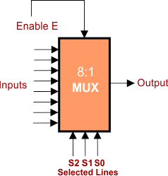
- Three select lines (S0, S1, and S2) for seven inputs to the multiplexer are shown in the following diagram.
Following is the descriptive diagram of 8×1 (8:1) multiplexer
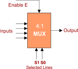
The descriptive diagram of 4×1 (4:1) multiplexer is given below
Important Points:
|
- Common Bus System uses a multiplexer to implement Common BUS.
- Six registers named AR, PC, DR, AC, IR, and TR and a memory unit connected to the common bus. The data register (DR) is also associated with the ADDER and Logic Unit to perform operations on data through the data bus.
- Input register (INPTR) is not connected to the common bus. It receives data directly from the input device, sends it to the Adder and Logic unit (part of ALU) for operations (+, -,*, /), and then passes it to the Accumulator register. Adder and logic unit has a carry bit called “E” in case of addition.
- OUTR Output Register does not send data to a common bus or any other register because it sends directly to the output device. But it receives data from the common bus.
Important : The common bus system connects every register with Clock Signals. Clock Signal controls LD, INR (increment), and CLR (Clear register) commands by the control unit. The Control Unit also controls memory read (R) and writes (W) operations.
Registers and Memory Size In Common Bus System?
Major points about memory and registers and their sizes in common bus system are explained below
- The Main memory is of 4096×16 = 2^12 x 16. To represent 4096 (2^12 ) memory, we require 12 bits. So, 12 bits are needed to address 4096 memory. We are multiplying by 16, which means that the size of the word is 16 bits. We need word size when we access or transfer data in memory and registers.
- We need the common bus size to be 16 bits because the word size is also 16, which must pass through the common bus.
- AR and PC registers work with memory addresses, so their size is 12 bits. When the address of these registers arrives at a common bus, its four most significant bits become zero.
- DR, AC, IR, and TR registers work with memory data, so their size is 16 bits, which is the size of a word.
- The input register (INPR) and the output register (OUTR) send and receive data character by character. Eight bits are required to represent a character. So, INPR and OUTR registers needed 8 bits. These registers communicate with the 8-least significant bits on the common bus
- The number of select lines required depends on the number of input components connected to the bus. Select lines follow the rule of 2^n, where n is the select-line bit-value. 2-bits can represent four components (0-3). Similarly, 3 bits are required to describe eight components numbering from 0 to 7, and so on
How Common Bus System Works?
Step I: Any register can send data to a common bus by activating its selected lines (S2, S1, S0).
Step II: If any register wants to receive data, its LD command will activate by setting the LD command value to 1. Set the LD command to zero for all other registers.
Note: The control unit manages the activation/deactivation of LD, INR, or CLR for any register.
Step III: The primary process starts with the program counter.
- The program counter retrieves the memory address for execution. Then, pass this address to the common bus.
- AR receives the address from the common bus by activating its LD bits. Then, AR sends the address to memory directly because AR connects to the common bus.
- Memory reads the address and sends data from that address to DR through a common bus.
Remember: The other names of DR (data register) are MBR and MDR.
Step IV: Memory-fetched data will be in the data Register and then passed to the Accumulator register by Data BUS because DR is directly connected with AC by the Data Bus. Copy of this data is transferred to IR because when data passes to the accumulator register, the Data Register will flush out. If the Accumulator register wants to hold (received data from DR) temporarily somewhere, it passes it to the Temporary register (TR). If we want to retrieve the data from TR, then its data is first loaded in DR, and then it passes to AC.
Common Bus System Example
Suppose one address instruction is
X= (A+B) * (C+D)
To execute the single-address instruction, the system performs seven micro-instructions as follows.
LOAD A // AC <– M[A]
ADD B // AC <– AC + M[B]
STORE T // Store AC value in the temporary register
LOAD C // AC <– M[C]
ADD D // AC <– AC + M[D]
MUL T // multiply temporary register value with AC
STORE X // Store value of X in memory
Explanation of micro-instructions
As the program loads, the Program counter gets the address of the first instruction. For example, the first instruction is LOAD A. LOAD A means load value A to the Accumulator register. The steps will be.
1. The first micro-instruction is LOAD A
It means to load the value A to the Accumulator register.
- The program counter (PC) gets the address of this instruction. The program counter has been activated by selecting the lines numbered 010. It transfers the address of an instruction to the common bus through the address register.
- The control unit activates the Address Register (AR) LD command. In this way, AR gets the PC’s address through a common bus.
- The Address Register (AR) is directly connected to the main memory.
- When the instruction address arrives at the main memory, the READ command of the main memory will activate, and data of the provided address is transferred to the common bus through the data bus.
- Now, activate the LD command of the data register. DR gets data from the common bus through the data bus.
- Copy the instructions in the MDR to the CIR. Data coming from memory (READ) or going to memory (Write) is always in the Memory Data Register MDR (DR or MBR). Fetch the instructions complete here, and now the PC is Incremented by ONE. It means the Program counter now has the address of the next memory location in the sequence.
- Transfer data from MDR to the control unit (ALU section) and decode it.
- Operator/opcode (i.e., ADD, LOAD) is separate from Operand (data, i.e., A) in the decode section.
- Transfer data to the accumulator register by passing through the ALU (for operations like +, -) via a data bus.
- Here is the completion of the first micro-instruction.
2. The second micro-instruction is ADD B.
This instruction means that ADD the value of B with the accumulator register value in the Accumulator Register.
- The value of “A” is already in the accumulator register; now, “+ B” arrives through STEP 1-7. Keep in mind in the first instruction execution, there was no need for the ALU section, but in the ADD B instruction, ADDER and LOGIC-Unit perform addition first and then pass the value to AC Register.
- Therefore, the value of AC will now be A+B.
3. The third micro-instruction is Store T.
It means storing the result of the Accumulator in a Temporary register (T). For this, AC will activate through its select lines and pass data to the common bus.
The LD command of TR will be activated through the control bus of the control unit. It gets data from the AC Register in a common bus.
4. The fourth and fifth micro-instructions are LOAD C and ADD D.
These instructions will execute like LOAD A and ADD B. Till Here, the Accumulator register (AC) has the value of C+D.
5. The sixth micro-instruction is MUL T.
It means multiplying the value of the Temporary Register (T) by the Accumulator Register. For this purpose, temporary register data is activated through select lines and passed to the common bus. The control unit activates the LD command of the DATA Register to get data, and DR receives data from the common bus and then passes it to the Accumulator Register. So now, in AC is (A+B)*(C+D).
6. The Seventh micro-instruction is STORE X
You can now store the value of AC in memory. So, the seventh micro-instruction is STORE X. It means storing the Accumulator Register’s value (in the X variable) in the main memory at the given address. Activate AC through its select lines. Pass AC data to the common bus and MDR through the data bus. Now, the memory Write command will be activated through the control unit, and memory gets data MDR and stores value in the X variable.
Note: If the user wants to display the results on the Monitor, then micro-instruction (Display X) can be used, which means that it loads the value of X from memory in the Data Register and then passes it to the Display device (output device).
Advantages of Common Bus System
Suppose we use wires to define the path of each register to everyone with other registers and memory (like in Mesh topology).In that case, common bus system is an efficient way to transfer data from one register to other registers and main memory.
Note: The implementation of common bus system is too complex, costly, and challenging.
Essential Points in the Common Bus System
- The question is how the data moves from the input device to an output device. The answer is that when we pass data from the input device (keyboard, mouse), it will go directly to INPR (input register), pass it to ADDER and LOGIC unit, and then move to AC. AC passes it to a common bus, and from the common bus, OUTR receives data, which then passes to the output device to display.
- If we use only the Address register (not the program counter register), then the Address register doesn’t know what to execute next. And it doesn’t know the location of the next instruction. It forgets the memory location after completing the first instruction. PC keeps the address of the next instruction in the sequence of addresses.
- Memory-fetched data will be in the DATA Register and then passed to the Accumulator register. When passing data to the accumulator register, clear the Data Register. To ensure the storage of the next incoming data. If the Accumulator register wants to keep this data somewhere temporarily, then it passes it to the Temporary register (TR). If we want to retrieve the data from TR, then its data is first loaded in DR and then passed to AC.
- If we use only the Address register (not the program counter register), then the Address register doesn’t know what to execute next. And it doesn’t know the location of the next instruction. It forgets the memory location after completing the first instruction, and then the PC keeps the address of the next instruction in the sequence of addresses.
- The DR is a two-way register because data going to memory or coming from memory will always be in the DR register.